Practical Reversing: Fanlight 02 - MCU ID and Debug
Last Time...
In the last post, I covered the acquisition and initial teardown of the DXTEEN pen light. You can find that post here. As a quick recap, we have access to a fairly well labelled PCB with a single primary MCU on it. We would really like to get insight to the code running on that MCU.
What is SWS?
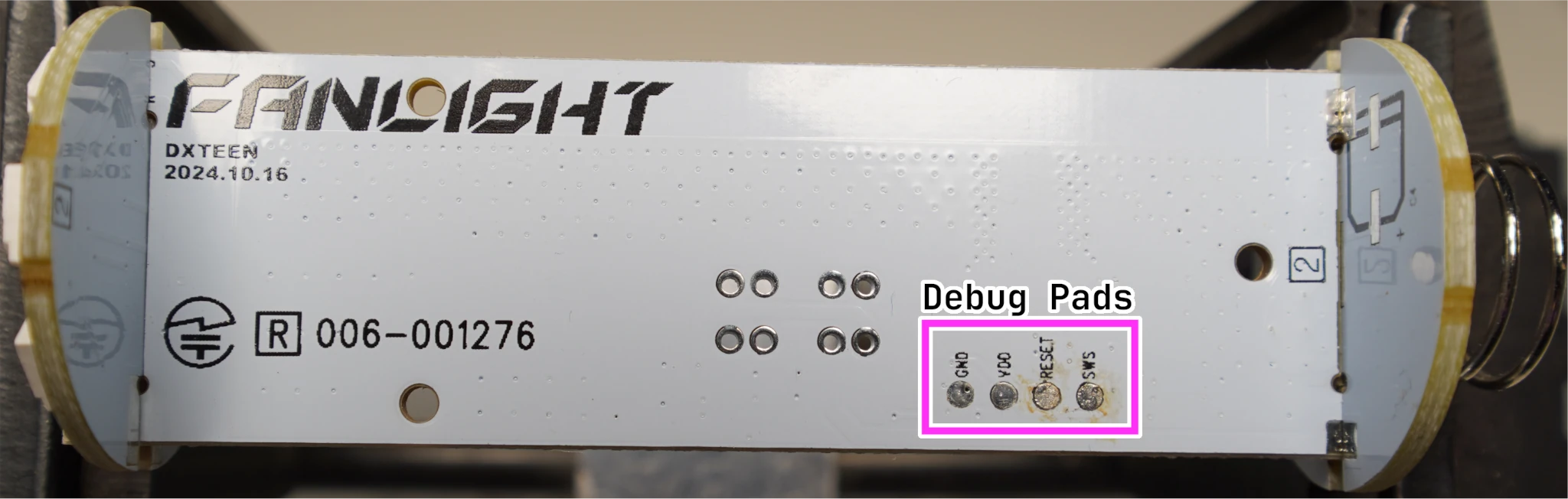
So what is SWS? I have no idea!
I've toyed with many ARM-based processors that use the very
common SWD interface.
This doesn't look like that, as there isn't nearly enough pins here. For one,
there's no apparent clock line. We have a suspicious cast of GND, VCC, and
RESET which are all very debug-friendly. Having a single pin present for SWS
hints at this being a single wire debug interface.
A quick search for SWS points to this very helpful GitHub repository. This is an implementation of the "Telink SWS Protocol" that runs using the PIO modules of an RP2040. Developers can build and flash this firmware to an RP2040 devkit. Then, the devkit will function as a debugger for these Telink parts. The project supports a handful of useful commands for us, including flash reading and writing.
At the time of this writing, the GitHub page further points to two additional resources that expand upon what SWS is and how it works, which includes rbaron's lovely writeup on a fitness tracker. I strongly suggest giving it a read.
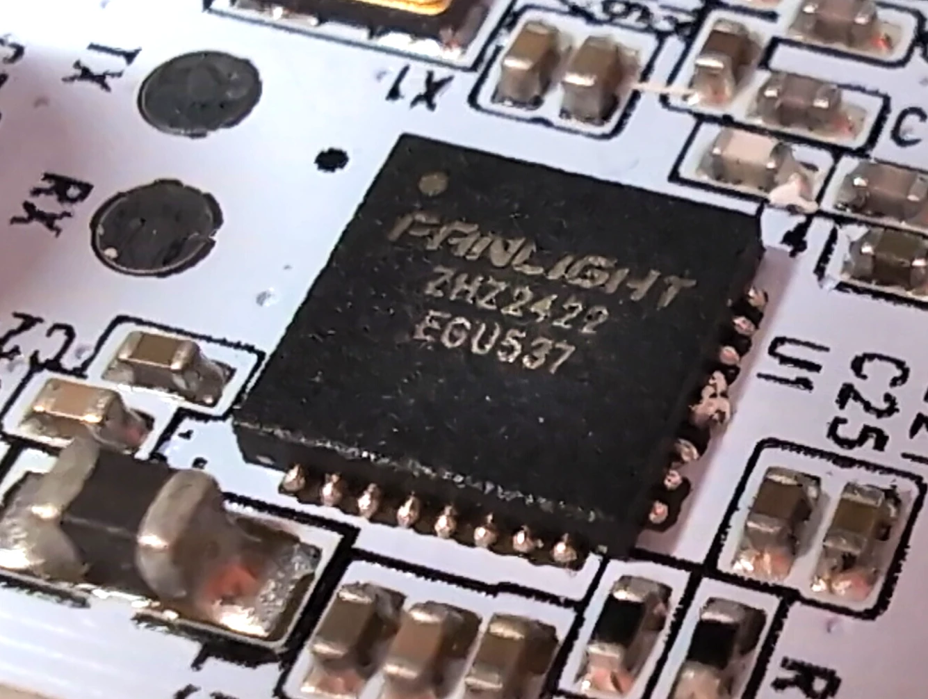
As a reminder, the SWS interface should lead to the single microcontroller on the board. If we take a closer look at the MCU, we see that the identifier printed on it is as follows:
FANLIGHT
ZHZ2422
EGU537
It's not labelled as a Telink part, but Fanlight doesn't make MCUs.
So could this be a Telink in disguise? Looking over the
davidgiven's GitHub repo
there is a nice get_soc_id command that Telink's SWS protocol supports. If we get
something sensible back from this command, it likely means we have a re-badged Telink part.
From there, we should have general debug access using this tool.
Building our Debugger
The telinkdebugger project is built to use PIO modules. This should mean that any
RaspberryPi processor with these modules can run it. The original developer was using an RP2040.
I recently helped The KoiBots set up an LED subsystem for their robot. That project left me with an abundance of these
RP2350-based Plasma boards.
The RP2350 has a similar architecture to the RP2040, and so porting to my devkit was very easy.
The pico-sdk project is a joy to use, and I continue
to recommend the RaspberryPi embedded line to anyone interested in embedded development.
I only had to change the PICO_BOARD CMake variable,
which already had an option for my board. As their docs state, you can see
a listing of the supported boards via the listing here.
diff --git a/CMakeLists.txt b/CMakeLists.txt
index 355c4ab..4467391 100644
# Generated Cmake Pico project file
-cmake_minimum_required(VERSION 3.5)
+cmake_minimum_required(VERSION 3.10)
set(CMAKE_C_STANDARD 11)
set(CMAKE_CXX_STANDARD 17)
set(PICO_SDK_FETCH_FROM_GIT ON)
set(USERHOME $ENV{HOME})
-set(PICO_BOARD pico CACHE STRING "Board type")
+set(PICO_BOARD pimoroni_plasma2350 CACHE STRING "Board type")
# Pull in Raspberry Pi Pico SDK (must be before project)
include(pico_sdk_import.cmake)
I also had to make a small modification to the src/telinkdebugger.cpp file to
set SWS and RESET to convenient to solder pins on my board.
diff --git a/src/telinkdebugger.cpp b/src/telinkdebugger.cpp
index 5699a0e..9502984 100644
#include <stdio.h>
#include <stdlib.h>
#include <tusb.h>
+#include "boards/pimoroni_plasma2350.h"
#include "pico/stdlib.h"
#include "hardware/pio.h"
#include "hardware/clocks.h"
#include "sws.pio.h"
#include "globals.h"
-#define SWS_PIN 2
-#define RST_PIN 3
-#define DBG_PIN 4
-#define LED_PIN PICO_DEFAULT_LED_PIN
+#define SWS_PIN 27
+#define RST_PIN 26
+#define DBG_PIN 7
+#define LED_PIN PLASMA2350_LED_G_PIN
#define SM_RX 0
#define SM_TX 1
Now, we can wire everything up together and provide power to our device under test.
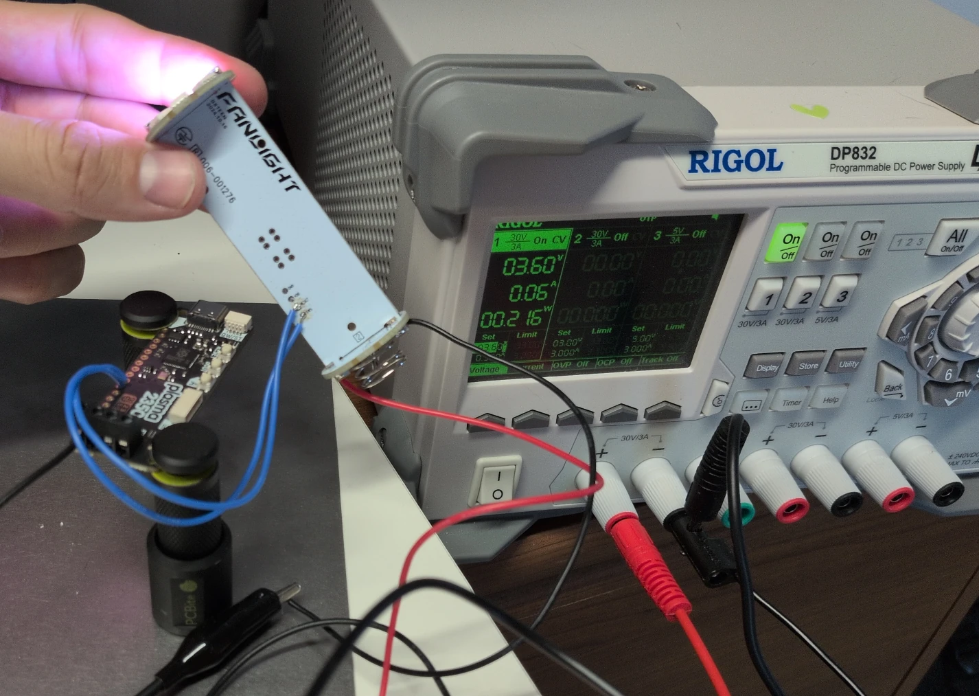
Now for the moment of truth...
MCU Identified!
So, this MCU does appear to be a Telink. It properly, consistently, and sensibly responds
to the get_soc_id command. So which Telink is it?
To the best of my knowledge, pvvx's script here is accurate. It appears that this MCU is a TSL8253. Following are some useful links for the part:
Our next immediate goal is to siphon off any data that we can from the chip. This should give us more insight in to how the device functions, maybe we can patch it to change what it does.
The telinkdebugger project supports the SWS commands to read and write data at arbitrary
addresses. Reviewing the datasheet above, the following address ranges look useful:
| Region | Start Address | Stop Address | Length |
|---|---|---|---|
| Flash | 0x00_0000 | 0x07_FFFF | 0x08_0000 (512 kB) |
| SRAM | 0x84_0000 | 0x84_BFFF | 0x00_C000 (48 kB) |
To support reading and writing these address ranges, I had to make another change to my fork of the project. The original author's target had 16-bit addresses. Here, we need 24-bit ones. Before this change, the board would not respond to my requests for data as I had not sent enough bytes over yet. After this change, we're able to read and write arbitrary memory just fine.
diff --git a/src/telinkdebugger.cpp b/src/telinkdebugger.cpp
index 5699a0e..9502984 100644
return pio_sm_get_blocking(pio1, SM_RX);
}
-static uint8_t read_first_debug_byte(uint16_t address)
+static uint8_t read_first_debug_byte(uint32_t address)
{
write_cmd_byte(0x5a);
- write_data_word(address);
+ write_data_byte(address>>16);
+ write_data_word(address&0xFFFF);
write_data_byte(0x80);
return read_byte();
return v1 | (v2 << 8);
}
-static void write_first_debug_byte(uint16_t address, uint8_t value)
+static void write_first_debug_byte(uint32_t address, uint8_t value)
{
write_cmd_byte(0x5a);
- write_data_word(address);
+ write_data_byte(address>>16);
+ write_data_word(address&0xFFFF);
write_data_byte(0x00);
write_data_byte(value);
}
return strtoul(buffer, nullptr, 16);
}
-static uint16_t read_hex_word()
+static uint16_t read_hex_short()
{
uint8_t hi = read_hex_byte();
uint8_t lo = read_hex_byte();
return lo | (hi << 8);
}
+static uint32_t read_hex_word()
+{
+ uint32_t word = 0;
+ for (size_t i = 0; i < sizeof(word); i++)
+ {
+ uint32_t temp = read_hex_byte();
+ temp <<= (8 * (sizeof(word) - i - 1));
+ word += temp;
+ }
+ return word;
+}
+
void set_tx_clock(double clock_hz)
{
sws_tx_program_init(pio0, SM_TX, sws_tx_program_offset, SWS_PIN, clock_hz);
Now, we're ready to read the contents of Flash and SRAM.
Huzzah! These all look like pretty real strings to me. Some interesting things to note:
- Telink vendor name present in the binary (
Telink Remote) - Possible build timestamp (October 29, 2024 @ 16:11:23)
- Product name (
DXTEEN LIGHT STICK) - Possible keys?
hanamfanlightkeyhanambinfanlightedwinfanlightkey- Note all of these are exactly 16 characters
Getting Decompilation with Ghidra
It turns out that the TC32 architecture isn't quite ARM. And it's not quite something that Ghidra or BinaryNinja know how to decompile either. But, six years ago, two hackers worked on a processor specification for this architecture for Ghidra. They pushed their work to GitHub. See trust1995's repository here.
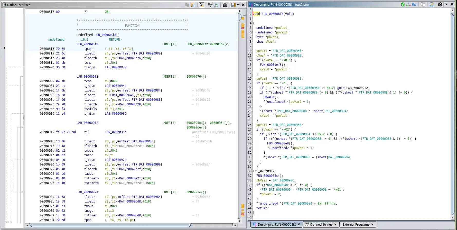
Using this processor spec allows us to get pretty solid decompilation out of Ghidra. We're able to get C-like assembly out and follow xrefs. If we add definitions for interesting memory locations present in the datasheet, we should be able to find regions of code that read or write to those addresses.
As an example, let's trace out PWM accesses.
What's PWM?
The Problem
Let's zoom out a bit and remember what we're hacking on here. All we really have is a BLE-enabled light stick. The core feature for this product is that it can display any RGB color that a fan would like. The light ring at the front of the device has 7 LEDs. Each LED has four segments corresponding to Red, Green, Blue, and White.
A fan would want to display arbitrary colors. If our MCU only supported on and off states for each LED, we'd be very limited in the colors we could display. We could maybe show just pure green. We could show green + blue to create cyan. We can't have different shades unless we can change the amount of red, green, and blue that we're adding.
We want arbitrary colors, not just fully green or fully blue.
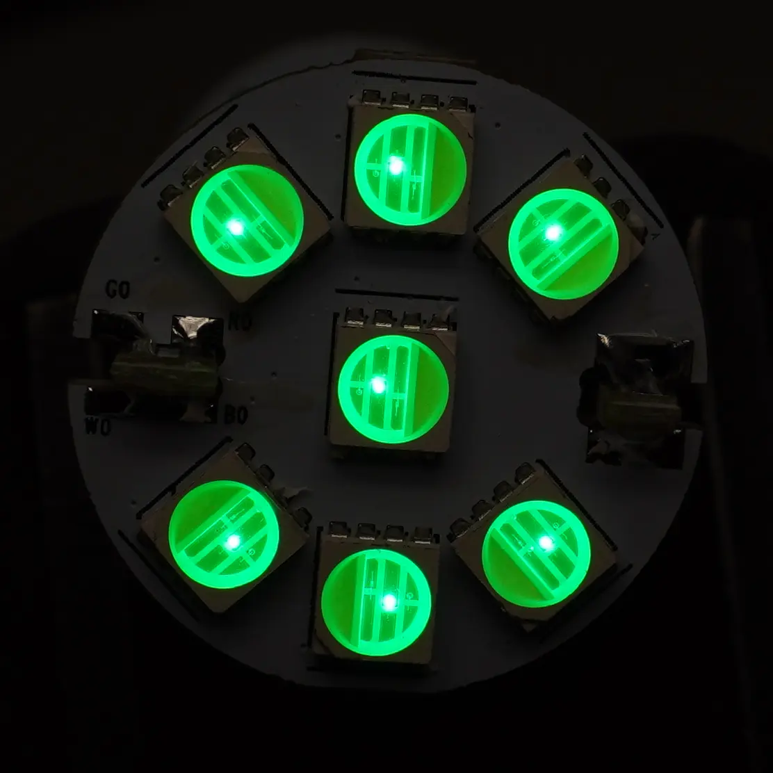
This is what PWM is going to answer for us. PWM stands for Pulse Width Modulation. Instead of turning, say, red on 100% of the time, we'll cycle it on and off at some (usually very fast) rate. So now we could create a color that's composed of 50%-power red, and 50%-power blue.
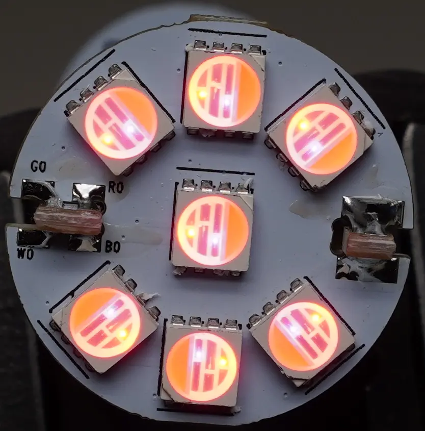
This is a very common feature to have available on an MCU. It's a standard way to solve this exact problem. The TSL8253 advertises support for PWM on specific pins. We should be able to verify if this is in use.
Verifying with Scope
Let's use a logic analyzer to peek at the signal reaching the LEDs to confirm that it's PWM.
Here again is the top side of the PCB.
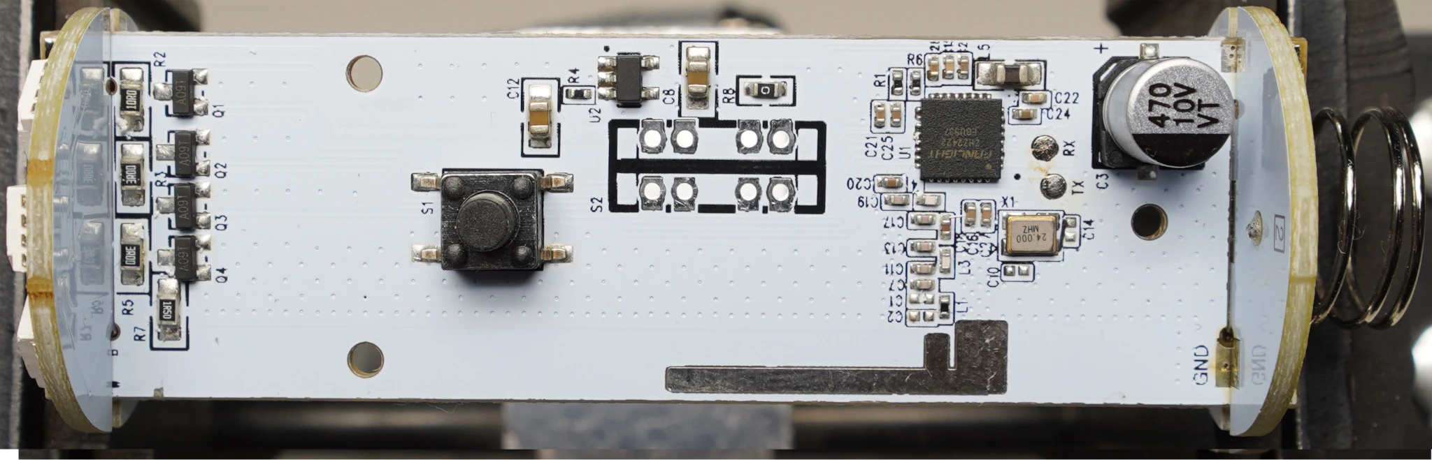
On the far left-hand side of this picture is the LED ring. Just before that we have a 4x repeating circuit
of transistor (Q1, Q2, Q3, Q4) and resistor (R2, R3, R5, R7).
![]()
These transistors act as a switch to turn on and off each color of our LED segments. There's 4 because the device drives red, green, blue, and white. All of the LEDs in the ring are wired together; there's a global signal for red, a global signal for green, and so on.
I'm spoiled and have a Saleae logic analyzer, but this next step could be done with Pulseview as well. I'm going to attach one probe of my logic analyzer to one of the transistors and monitor that signal. While recording that signal, I'll cycle through the LED colors.
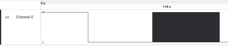
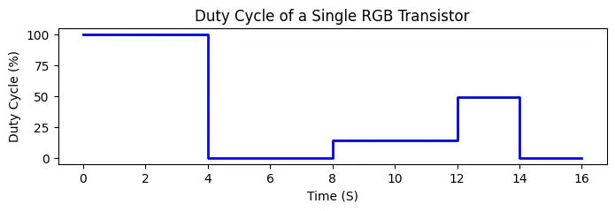
So over the course of 15 seconds, we see the signal transition through the following states:
- Fully on
- Fully off
- Some mix of on and off
- Back to fully off
If we zoom in on the "mix of on and off" section we see the following:
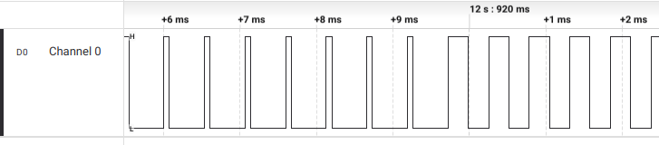
That certainly looks like PWM to me. We have a periodic signal with some defined rate. At this point in the recording we can see the widths of the pulses hit a transition. The "on" time goes from some smaller value on the left, to some larger value on the right.
We can use our logic analyzer's GUI to select these regions and measure their duty cycle. This tells us how often the signal is on for a given period of time.
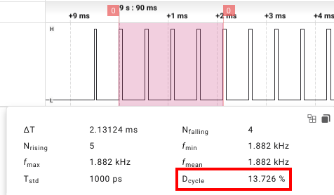
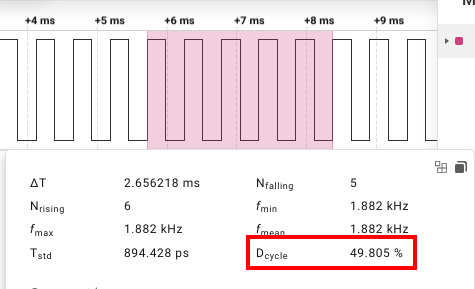
We can expand our previous state definitions now. We can qualify the "some mix of on and off" state to use specific duty cycle values.
Datasheet Crawling
So how'd the firmware do that? A developer wrote code to configure the PWM subsystem on the MCU. That developer would've used the SDK which itself is informed by the TSL8253 Datasheet.
The following figure shows the memory map for the TSL8253 as well as the start to the register table
for PWM. Both of these are just screenshots taken from the datasheet linked above.
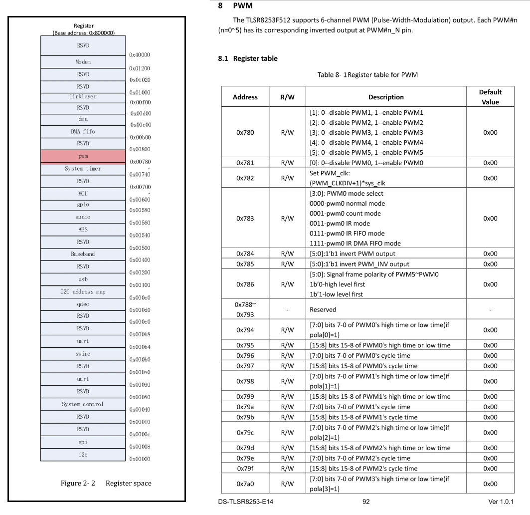
The Telink MCU, like most MCUs, is using a memory-mapped interface to provide an API for the developers. This means that every item that needs to get configured -- what the PWM mode is, what it's duty cycle is, etc, all are done by writing to memory.
So a developer might write some C code that looks like this to control a pin with PWM:
// Copied from pwm.h for clarity
typedef enum pwm_mode;
int
According the datasheet as provided, the following snippet of C code is equivalent. It would have the same behavior as the first sample.
// REGISTER_BASE_ADDR = 0x80_0000
// PWM_BASE_ADDR = 0x780
int
This is because those functions, pwm_set_mode(), pwm_set_pulse(), etc., are all wrappers around a memory mapped interface.
They compile to writes and reads of fixed addresses. When the architecture hits a write or read of those mapped addresses
they'll be forwarded along to the write block of hardware -- in this case, configuring the chip's PWM registers.
XRefs
So now back to Ghidra. We've identified, with a logic analyzer, that the MCU is using PWM to control its LEDs. We've reviewed the datasheet to get an understanding of how a developer would be coding to use this PWM feature. We also have a sense for what these function writes look like without abstraction -- just writes and reads to a known fixed offset.
With all of this knowledge together, and the binary in hand, we should be able to find the function that is actually setting the LEDs
pretty quickly. We can assume, for example, that something will need to turn the PWM module on.
According to the datasheet, that's accomplished by writing a 1 to bit position 0 at offset 0x00 of the PWM,
which corresponds to address 0x80_0780.
So let's give that address a sensible name in Ghidra and see what references it.
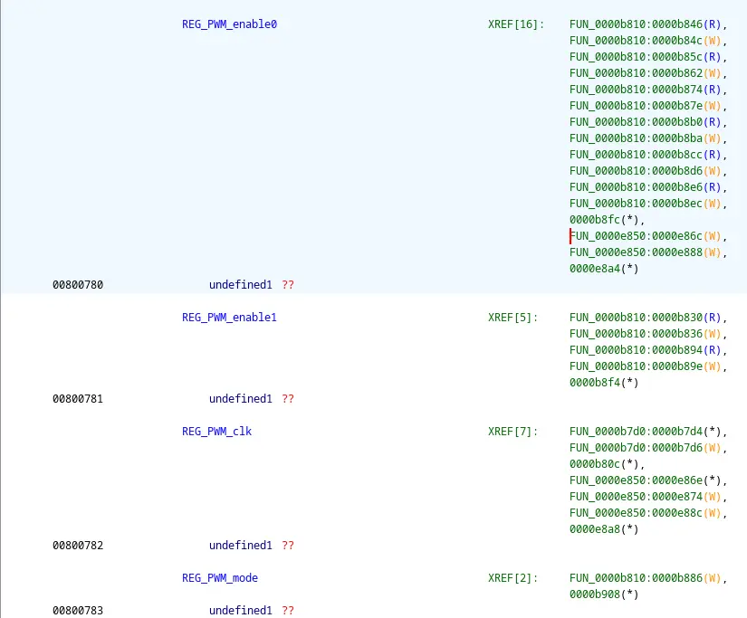
It looks like our PWM registers have quite a few xrefs!
So functions at the following addresses all do some amount of reading or writing in the PWM register space:
0xb8100xe8500xb7d0
Let's look at the first one on our list, as it has the most references for these registers.
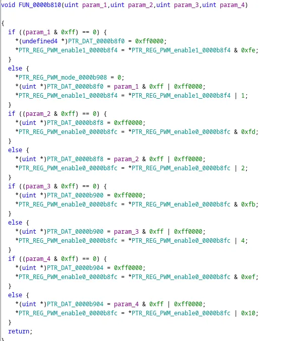
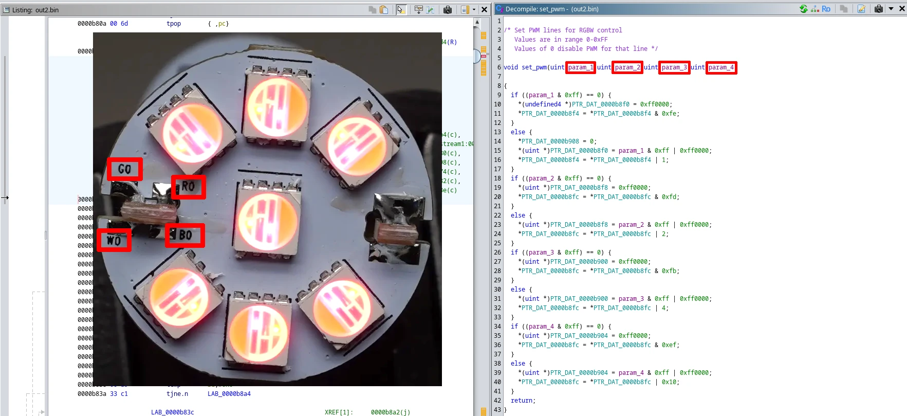
So what's this function doing? Each parameter goes through the same check and an equivalent assignment.
If the value passed in is 0, use an AND Bitmask
to disable a particular PWM line, and set some magic pointer to 0x00ff_0000. If the
value passed in is not 0, use an OR bitmask to enable a particular PWM line,
and set some magic pointer to the lower 8 bits of the value passed in, OR'd with 0x00ff_0000.
If we dig deeper on those "magic pointers" we'd find that they match offsets for the duty cycles for PWM0, 1, etc. The bit masking we're seeing around them is to due to the PWM registers being one byte each, but our writes being of size 32-bits, four bytes. Matching the relevant registers to a packed structure would look something like this:
;
The cycle time is always set to 0x00ff, and our high time within that cycle is some value in the range of
0x0000 to 0x00ff, depending on what the user provided. So we could say the function does the following
for each of the four parameters:
Is the value 0?
  If yes:
    - Disable PWM
    - Set cycle_time to 0xFF
    - Set high_time to 0x00
  If no:
    - Enable PWM
    - Set cycle_time to 0xFF
    - Set high_time to (value & 0xFF)
And that's repeated for each of the four parameters. Four parameters because:
Neat.
Patching the Binary
Now that we have a sense of how this section of code works and what it controls, let's see if we can change its behavior.
We should be able to patch the binary to just never turn on one of the LED colors. This
should be as easy as nop'ing out the register writes associated with one of the four PWM
modules in use.
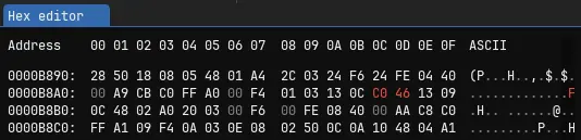
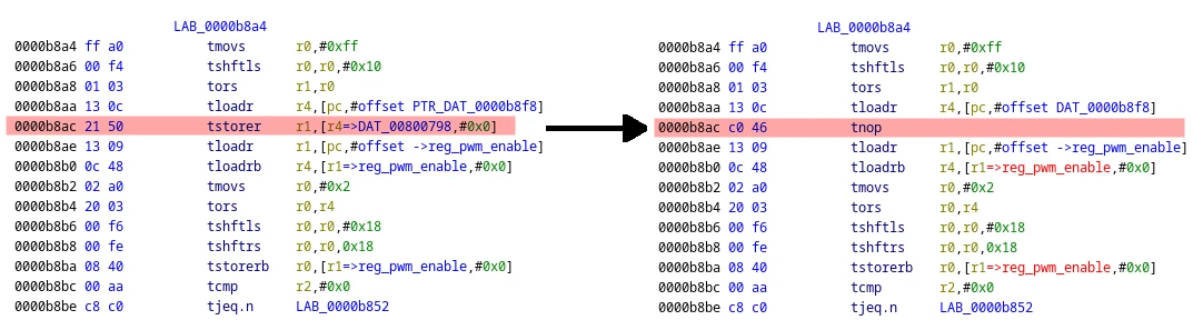
For this, we'll just need to do a small hex edit to change the tstorer instruction in to
a tnop. Ghidra's built in hex editor is fine, but I was also using the lovely ImHex
while working on this project, and so I made the edit there. We can see from other
places in the listing view that the opcode for a nop in this architecture is c046.
Here's a matching delta in Ghidra as well. This is a screenshot I took elsewhere in my notes, so the symbol names aren't an exact match from earlier.
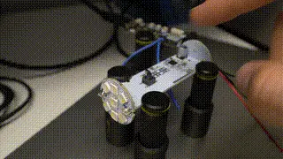
Let's flash this patched binary using our telinkdebugger utility RP2350 and see what happens!
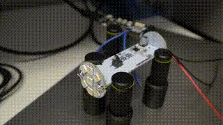
You might have to scroll back up to the original gif to compare, but our patch removed green! So we've learned the following things about the device:
- The function at
0xb810is responsible for driving colors param_2of this function controls the output for green- We can flash patched binaries back to the device
- There is no code integrity in place
3.1 here is really interesting for me. The binary contains some header and footer information that we'll
be covering in another blog post. One of these values appears to be a CRC, which had me worried that my
random monkeying around would trip up. It turns out that CRC is only checked when firmware is pushed over
bluetooth -- if at all.
Up Next
In the next article, I plan to write about additional exploratory work done on the BLE interface. No sick PoCs here, just some Android APK unpacking with JADX and some BLE exploration with WHAD.